
Graphene - a single atomic layer of graphite
the thinnest material known to man and maybe the next step in the world of superconductive materials
Erik Friebe
5/20/20243 min read
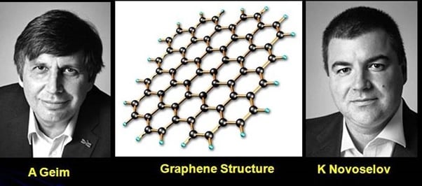
Graphene, a single layer of carbon atoms arranged in a hexagonal lattice, with a carbon-carbon distance of 0.142 nm, has been hailed as a wonder material since its discovery in 2004 by Andre Geim and his former student Konstantin Novoselov in the University of Manchester, England.
Six years later they received the the Nobelprize for their groundbreaking experiments on graphene.
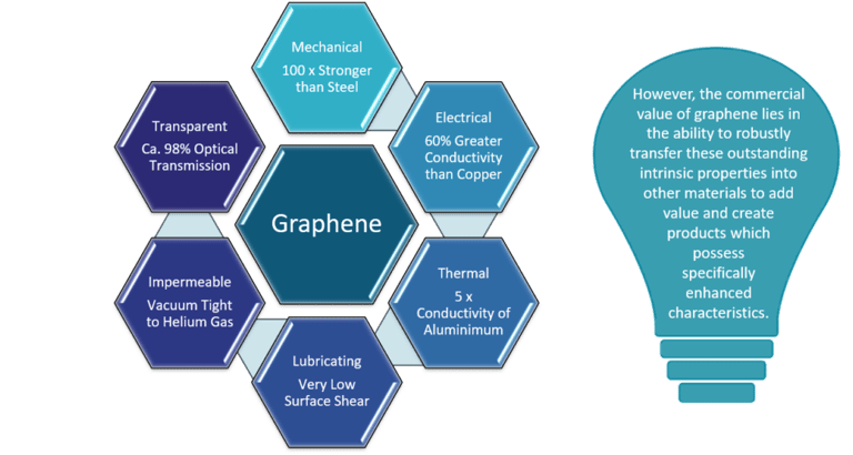
Properties
History
Electrical
Graphit (3D): 0,000 008 Ωm
Graphene (2D): 0,000 000 001 Ωm
Copper: 0,000 000 017 Ωm
Thermal
Graphit (3D): 150 W/(m•k)
Graphene (2D): 5000 W/(m•k)
Copper: 400 W/(m•k)
Mechanical
Graphit (3D): 4•10⁷ Pa
Graphene (2D): 1•10¹¹ Pa
Steal: 7•10⁸ Pa
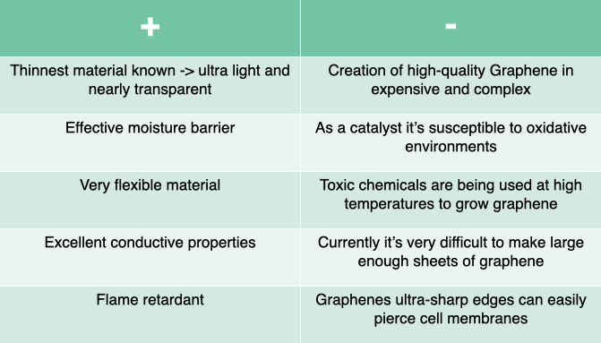
Pro's & Con's
Possible Usage
Electronics: Graphene transistors can potentially outperform silicon, leading to faster, more efficient electronic devices.
Energy Storage: In batteries and super capacitors, graphene can enhance capacity and reduce charging times, paving the way for longer-lasting and quicker-charging batteries.
Composites: Adding graphene to materials like plastics, metals, or ceramics can significantly improve their strength and durability.
Medical: Its biocompatibility and conductivity make graphene ideal for developing advanced medical devices, sensors, and even targeted drug delivery systems.
Sensors: Graphene’s sensitivity to various substances makes it perfect for creating highly accurate sensors for environmental monitoring, health diagnostics, and more.
Possible Application
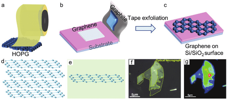
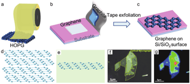
Micromechanical exfolation
peeling systematically ordered pyrolytic graphite with the use of adhesive tape
graphene is sliced into various flakes of few layers by continuously peeling the multi-layer graphene
not suitable for large productions and a homogeneous and precise application

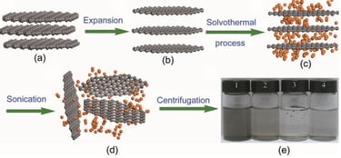
Liquid-Phase exfolation
using solvent like acetic acid, sulfuric acid and hydrogen peroxide, to exfoliate graphite through ultrasonication
used to create graphene nanoribbons, but large-scale growth of graphene is difficult task in this method
Chemical vapor deposition
in this process, nickel and copper used for large scale production of graphene
during the process film of metallic catalyst deposits on the substrate
chemical etching is performed on the deposited material on the substrate
after chemical etching, a mixture which containing the carbon is passed into the reaction chamber -> highest quality possible

Flame synthesis
widely used mass production method for making nano particles
method is not well adopted for production of graphene as compared to chemical vapor deposition
has potential to produce graphene economically

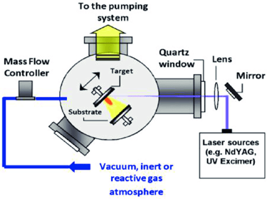
Pulsed laser deposition
laser energy source is outside the chamber; and chamber is maintained ultrahigh vacuum
material is deposited by at an angle of 45° by stoichiometry transfer between ablated target and substrate material
substrates are added to its surfaces parallel to the target at distance of 2–10 mm
main advantages is low temperature growth rate achieved such that high-quality graphene made without defects
Extra: Twistronics
Chances of combining 2D-Materials to build a 3D-Material -> will create Interfaces wich can have interesting functionalities (similar to pn-junction)
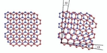
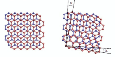
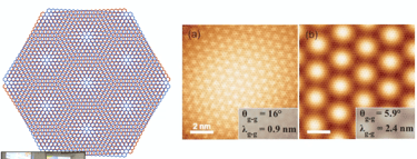
Moiré-patterns on atomic scale when combining two layers of graphene in an angle of 16° and 5,9°
-> the pattern mirrors the hexagonal structure of carbon atoms

The „magic“ angle of 1,1°
Two layers of graphene can conduct the electron without any resistance
This can be accomplished by twisting these two layers at 1,1°
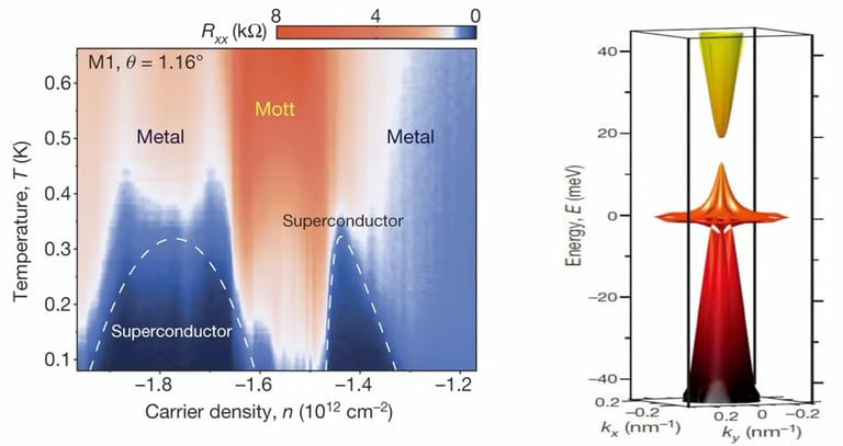
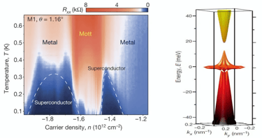
Reason for superconductive properties of bilayer graphene with an angle of 1,1°